
Équipe PM2E
Propriété des Matériaux pour les Économies d’ÉnergieResponsable d’équipe : Alexandre VIVET
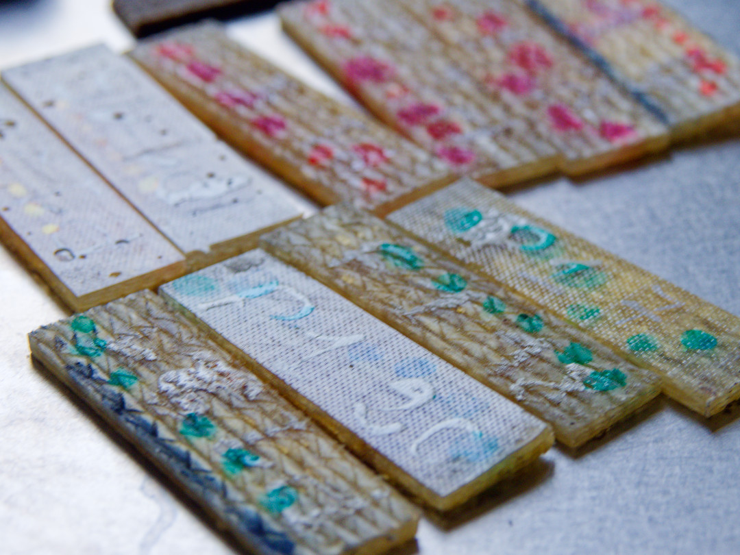
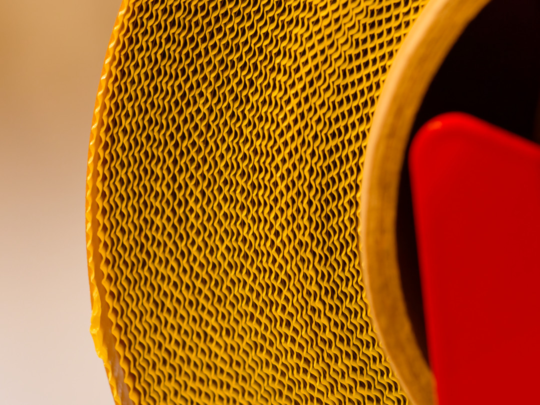
L’équipe PM2E s’intéresse aux interactions entre les procédés de fabrication, la microstructure et les propriétés d’usage des matériaux, avec pour objectif d’optimiser le cycle de vie des structures et dispositifs, par réduction des consommations énergétiques et utilisation de matériaux bio-sourcés. Le champ de recherche de PM2E va des matériaux semi-conducteurs aux matériaux composites. En couplant des investigations et observations et des méthodes de simulation à différentes échelles, les chercheurs de l’équipe PM2E apporte une compréhension fine des phénomènes en jeu durant toute la vie de ces matériaux.
QUELQUES CHIFFRES

MOTS CLÉS
LES AXESDE RECHERCHE
LES MEMBRES DE L'ÉQUIPE
MEMBRES PERMANENTS
Marie-Pierre CHAUVAT
Jun CHEN
Germain CLAVIER
Florian GEHRING
Viwanou HOUNKPATI
Magali MORALES
Christophe POILÂNE
Pierre RUTERANA
Mohammed SAHLI
Alexandre VIVET
MEMBRES NON PERMANENTS
El Hadji Amadou BA
Huaping LEI
Rofka RAMDANI
Ayla ZAITER